Surface polishing technologies - Essential technologies for semiconductor, MEMS, and LED manufacturing
Manufacturing of ultra-small sensors using Micro-Electro Mechanical Systems (MEMS) technology and Light Emitting Diode (LED) chips has continued to advance in recent years. These components are indispensable for a wide range of precision and communications equipment prevalent in today’s world. One of the key technologies that make the manufacture of such components possible is ultra-high precision surface polishing technology.
Table of contents [close]
Wafers require high precision surface polishing
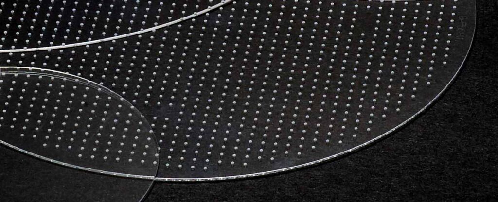
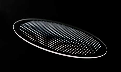
In the manufacture of semiconductor devices, a thin silicon wafer is put through through a series of processes such as sputtering, etching, and photolithography. After the semiconductors are formed, the wafer is diced to release each device. Each individual device is then wired and packaged to become the final semiconductor device. LED devices are manufactured in a similar way. Gases that contain nitrogen and gallium are sprayed in a chamber and allowed to react and grow gallium crystals, forming a large number of LED chips on a single sapphire substrate.
To ensure consistency and precision of the semiconductors, the silicon and sapphire substrates must be extremely flat and polished to a mirror finish. For this, high-precision surface polishing is required. Without adequate polishing, the devices will be misaligned and distorted, making it impossible to achieve the required nano-level accuracy and reliably.
For MEMS devices, in which integrated circuits and mechanical structures are placed on top of the semiconductor wafer, room temperature bonding methods are used. Room temperature bonding uses the atoms of the objects to be joined to fuse the joint without using heat or adhesives. Room temperature bonding is also widely used in the manufacture of Silicon on Insulator (SoI) wafers, which are often used to manufacture MEMS devices and high-performance semiconductor components such as CPUs. Materials that are typically difficult to join, such as sapphire, diamond, ceramics, and various metals, can be joined using the room temperature bonding method. Since the connections are made without heat or adhesives, even materials with different thermal expansion properties can be joined without warping or other issues.
Room temperature bonding requires high-precision surface preparation to achieve flatness at the atomic level for each material that is to be bonded. Therefore, high-precision polishing of the materials is required.
Surface polishing methods
Abrasives and slurries made of a high-hardness material such as diamond are used for surface polishing. Materials are polished by pressing a polishing pad made of a material such as urethane against the material to be polished and rotating the pad while feeding the abrasive or slurry. In order to polish efficiently, polishing is done in stages from rough polishing to medium polishing to finish polishing.
The final finishing stage for hard materials such as sapphire and ceramics is accomplished by Chemical Mechanical Polishing (CMP). Surface polishing with CMP is widely used in the semiconductor industry for polishing wafers made of hard materials such as silicon carbide (SiC) and gallium nitride (GaN), as well as for polishing sapphire substrates for LEDs. Atomic level precision polishing of wafers and materials using CMP is necessary prior to performing room temperature bonding.
CMP uses a combination of chemical compounds contained in the slurry to slightly soften the substrate and minute abrasives to polish the softened surface. This increases the mechanical surface removal effect of the abrasive grains in the slurry and results in a flatter and smoother surface. CMP allows for selective polishing of surface materials by adjusting the chemical composition of the slurry. The surface texture can also be controlled at the atomic level. For example, CMP can be used to polish the surface of a sapphire substrate to create steps exactly one atom high at regular intervals. This enables uniform epitaxial growth of GaN, which is used to create blue LEDs.
Technologies that make high-precision polishing possible
Polishing results vary depending upon the slurry used, polishing force, rotation speed, and many other parameters. Each material and application has unique polishing requirements. The combination of parameters is nearly infinite, only a few of which are optimal for each application. Therefore, polishing skill, experience, and knowledge of the many materials, applications, and polishing conditions are necessary in order to find the optimum combination of polishing parameters.
In addition to smoothening the surface, polishing must also flatten the overall shape of the substrate. Flatness down to the atomic level is required for room temperature bonding of high-performance semiconductor and MEMS devices. High-precision surface polishing requires both advanced polishing and flattening techniques. In particular, materials such as diamond and sapphire, which are often used in cutting-edge precision equipment and communications equipment, are difficult to polish. Advanced technology and significant proficiency are required to perform surface polishing on these materials.
Contract Processing of Orbray

Orbray's Sapphire products

-
Award: Industrial Standardization Enterprise Award
-
What is the Sapphire?

-
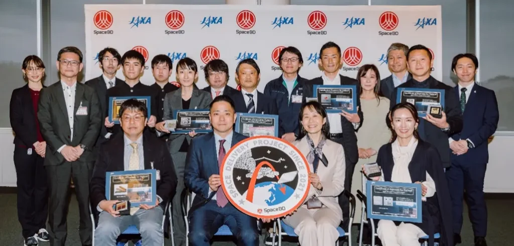
First round of Space Delivery Project “RETURN to EARTH” The ceremony celebrating the return of the payload items was held
-
Jewel bearings: Orbray and the watch industry [Story of Watch 1]

-
Industrial applications of sapphire

-
Pioneering the Future of Multi-Core Optical Fiber Connections : Orbray's Optical Fiber Bundling and Light-Induced Self-Written Optical Waveguide Technology