Diamond is the ultimate material which has the best physical properties of all materials in terms of hardness, acoustic velocity, thermal conductivity, Young's modulus, etc. Additional properties include transmittance of a broad wavelength spectrum from ultraviolet to infrared, thermal and chemical stability, and controllable electrical resistance/conductivity. These properties make diamond useable in a variety of applications, such as heat sinks, machining tools, optical components, audio components, and semiconductors.
Diamond Production Method
The present diamond synthesis method is high-pressure, high-temperature (HPHT) method. The homoepitaxial diamond growth process on HPHT-diamond substrate by Chemical Vapor Deposition (CVD) is also well known method for producing diamond substrate. This method is superior in the quality but limits the substrate size.
World's first, large diameter diamond production method
Orbray employs Heteroepitaxy targeting large diamond substrates.
In principal, hetroepitaxy, which uses a foreign material as a basal substrate, has theoretical possibility
of producing diamond substrates with the same size as basal foreign substrates.
However, due to the heteroepitaxial strain owing to the lattice and thermal expansion differences of diamond
and basal substrate, quality degradation and crack generation still occur in thick bulk diamond growth.
We made a new approach to overcome the above mentioned issues in heteroepitaxy. Based on the world's first
Ir/Sapphire basal substrate process technology, we
combined with our own newly developed microneedle growth technology (JP Patent 6142415B) which enables to
prevent crack generation and allow to grow stress-free, high quality, large diameter diamond substrate for
stable production. The diamond wafer has been named KENZAN Diamond™.
In addition, a novel step flow growth technology was developed to grow two-inch (50 mm) diameter diamond
crystals which are needed for industrial applications. We capitalized on our sapphire substrate technology to precisely
control the base sapphire wafer. The inclined Ir/sapphire surface results in lateral growth of the diamond
crystal, which alleviates stress accumulation during the growth process. We are now tackling the challenge
of further increasing the wafer size, with four-inch diameter as the next stage.
Fabrication technique of KENZAN Diamond™
Novel technology (Step-flow growth)
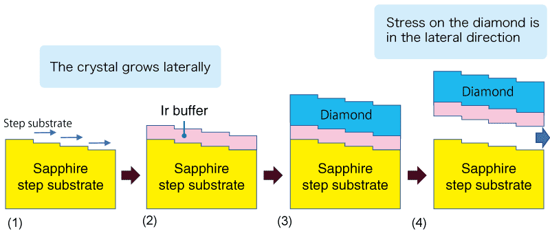
Simple manufacturing process leads to cost reduction.
Conventional technology (Microneedle growth)
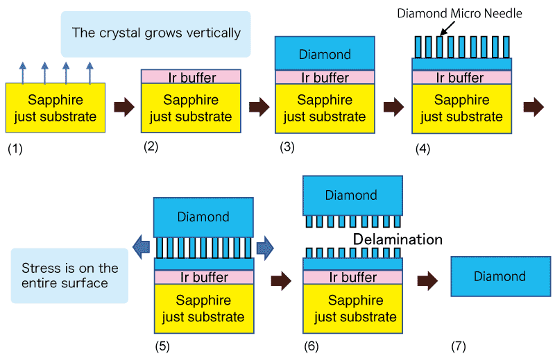
Conventional structure
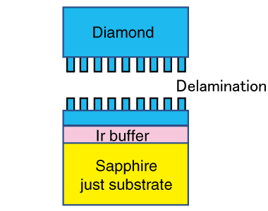
- A large amount of stress is applied to the grown diamond, causing cracks.
- Microneedles are needed to prevent the diamond from breaking.
- Microneedle fabrication process was complex and costly.
Novel structure
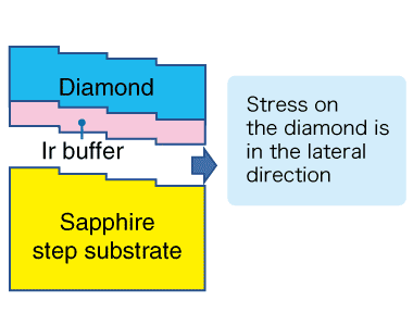
- Step flow growth uses sapphire step substrate.
- Stress on the diamond layer is applied laterally, eliminating the need for microneedles.
- Significant reductions in production time and cost make step-flow growth an appropriate technique for mass production. Two-inch diamond substrate is available.
Related Information (Blog)
- What are Diamonds?
- What are Diamonds?: Synthesis of Diamonds
- Novel Diamond Semiconductors Operate at Highest Power Ever
- Method for mass production of 2-inch diamond wafers developed – Expected to spur industrialization of power-semiconductor devices
- Two-inch
high-quality (001) diamond heteroepitaxial growth on sapphire (11
 0) misoriented substrate by step-flow
mode(Applied Physics
Express)
0) misoriented substrate by step-flow
mode(Applied Physics
Express) - Success in mass production technology for ultra-high-purity 2-inch diamond wafer; expected to spur realization of quantum computing NEW!

