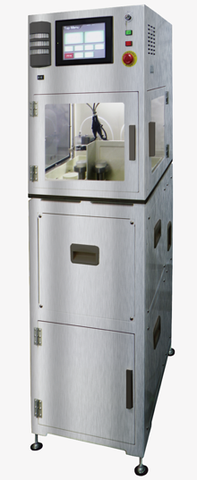
Wafer Cleaning System
Orbray’s wafer cleaning system - the world's first cleaning tool enabling high quality cleaning and drying for wafers less than 2 inches in diameter.
Until now, cleaning for new materials, such as small crystals or wafers less than 2 inches in diameter, has been limited to processes such as dip cleaning, resulting in unsatifactory cleanliness. Because of this, it has been a challenge to make devices that are able to utilize these new, advanced materials to their full potential.
Our wafer cleaning system has been built on Orbray's own cleaning know-how, developed through the manufacturing of sapphire wafers for LED applications, and features a newly-developed, original cleaning/drying mechanism for small-sized wafers. With these new functions, our wafer cleaning system has a capability of high level cleaning and solves the previous issues of cleaning, which had become an obstacle in the development of these new, advanced materials.
Through Orbray’s wafer cleaning systems, we strongly supports the development of new advanced materials and manufacturing of related devices.
Features
Original Scrubber Cleaning System
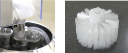
High-efficiency particle removal is achieved without causing surface or subsurface damages.
Drying System
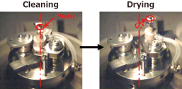
High quality of drying for small wafers is achieved with decentering spin dryer.
Patent No. WO2015-098699
Customizable Functionality
Able to customize according to specific needs.
Applicable Objects
- Single crystal (GaN, SiC, AlN, Sapphire, Diamond)
- Optical glass
- Biochip
Features
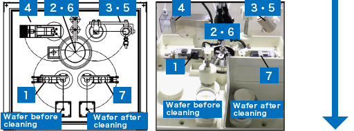
- Wafer transportation
- Vacuum chuck
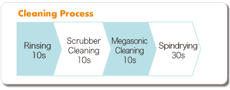
- Rinse (with pure water)
- Scrubber cleaning
(with cleaning solution) - Megasonic cleaning
- Spin dryer
- Wafer transportation
Example of cleaning results
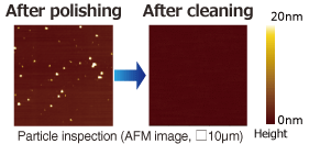
<□5mm Sapphire substrate>
<□5mm GaN Substrate>
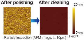
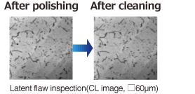
Particles were removed after cleaning without formation of latent flaws.
Lineup
Orbray is also providing contract wafer cleaning service.
| Product name | Wafer cleaning system |
|---|---|
| Cleaning process | Single wafer |
| Wafer size | □3mm, □4mm, □5mm, φ0.5”, φ1”, φ2” (φ3”, φ4”,φ6” are available. Other sizes are negotiable.) |
| Cleaning time using recommended process |
2min./wafer (loading to unloading) |
| Function | Wafer transportation |
| Scrubber cleaning (brush height adjustable) | |
| Mega sonic cleaning @950kHz | |
| Decentering spin dryer (rotational speed:~3,000rpm) | |
| HEPA filter (FFU) | |
| Dimensions (mm) |
480W x 600D x 1,680H |
| Weight (kg) |
200 |
| Utilities | Air pump (external): 0.5MPa or higher |
| DI water (recommended process): 400ml/wafer | |
| Power supply: 100VAC single-phase 1,000W |

