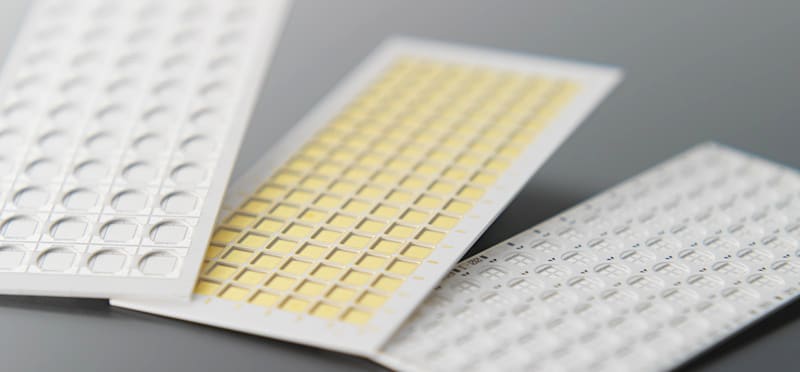
LTCC (Low Temperature Co-fired Ceramics) is a multi-layer glass ceramic substrate which is Co-fired with low resistance metal conductors at low firing temperature (less than 1000℃). It is sometimes referred to as "Glass Ceramics" because its composition consists of glass and alumina.
 (Zero Shrinkage LTCC)
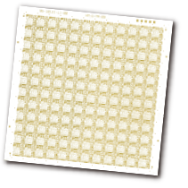
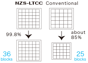
What makes Orbray's LTCC unique is its "Zero-shrinkage Sintering Process" which limits shrinkage to be in z-direction only. This process provides excellent dimensional accuracy and surface flatness. Orbray's LTCC also offers superb electrical characteristics thanks to its low dielectric ceramic materials and low resistance Ag conductors.
| Standard LTCC | NZS-LTCC | |
|---|---|---|
| Shrinkage Ratio | 15 | 0.2 |
| Tolerance | +/- 0.5% | +/- 0.05% |
Advantage
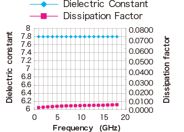
Stability in High Frequency
1GHz~18GHz!
Zero Shrinkage Ratio
More Parts After Firing!
High Accuracy of Shrinkage Tolerance
Suitable for Flip Chip!

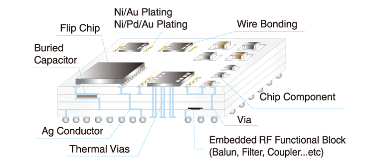
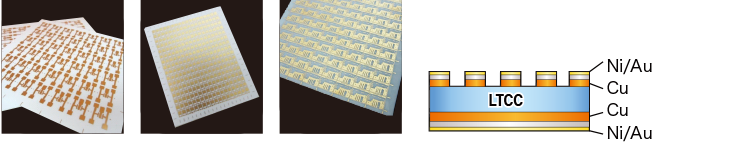
Embedded RF Passives

Direct Copper Plating Electro Ceramics
Cu : > 70um
Available for Alumina, AlN
LTCC Processing
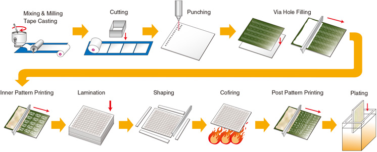
LTCC processing animation
Main Applications
- MEMS Sensor Package
- RF SiP/FEM Substrate
- Frequency Device Package
- Medical Equipment
- Industrial Equipment
- LED Chip Carrier
 (Hollow structure LTCC) <NEW!>
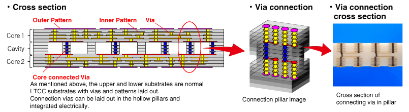
Using a process that differs from that of normal LTCC substrates, a hollow structure can be laid out in the substrate.
Not only is the hollow structure created, but everything apart from the hollow structure can be made conductive, successfully integrating the two.
In addition, the LTCC substrate sandwiching the internal hollow structure can be configured with pattern layout and via settings, just like a normal LTCC design.
Structure
A normal LTCC substrate with a hollow structure inside.
Supports a wide range of applications depending on the shape and layout of the hollow part.
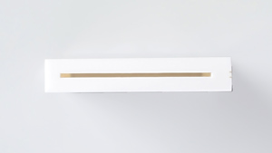
Appearance
The shape of the hollow part has a high degree of design freedom, so a variety of configurations are possible.
In addition, the substrate surface also has a high degree of flatness (exact value depends on the design values of each part).
As an example, for a hollow part with a height of 0.50mm, width of 150mm, and length of 70mm, the flatness will be within ± 20um.
| Measurement | 1 | 2 | 3 | 4 | 5 | 6 |
|---|---|---|---|---|---|---|
| Measured value | 15.0μm | 20.0μm | 12.5μm | 12.5μm | 20.0μm | 12.5μm |
Appearance details
The hollow part has high design flexibility, and can be designed according to request.
Via and pattern layouts can be handled at the same level as a normal LTCC substrate.
Hollow part
Since there is a high degree of freedom in design, it is possible to manufacture not only straight lines but also curves.
Therefore, a variety of shapes are possible for the hollow structures.
Via section of pillar
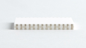
Pillar connection vias can be laid out, and components can be mounted on the top and bottom surfaces.
Corner section
Conductor layout is also possible inside the hollow part, so the substrate is suitable for various sensor parts and nozzles.
Advantages
Since the hollow part and conductor pattern can be laid out together, the substrate can support miniaturization and compound use in various applications.
It is also possible to reduce material costs and man-hours by integrating products that previously had to be configured using multiple parts.
Since the structure and the substrate are integrated, it can operate maintenance-free (fine adjustment, etc.), it's easy to handle, and work efficiency can be improved.
Application examples
- Nozzles that require conductors.
⇒ Nozzle for atmospheric pressure plasma cleaning equipment.
It is possible to appropriately design the internal conductor pattern shape and the distance between conductors depending on the type of gas used.
The shape for rectification at the nozzle tip is also available.
- Substrate utilizing the hollow as a flow path.
⇒ Sensor unit that analyzes gas and liquid components.
⇒ Substrate that resists high temperatures by the flow of cooling gas and liquid through it.
- Substrate with special characteristics, created by filling the hollow part with a different material.
⇒ Substrate with excellent high frequency characteristics.
⇒ Substrate filled with high shielding material to reduce signal interference.
⇒ High heat dissipation substrate filled with high heat dissipation material.
- Built-in integrated component substrate for miniaturization and space saving.
(Note: The mounting part requires an opening)
⇒ Component mounting, or built-in cavity substrate.
- Substrate that requires partial thermal insulation due to product configuration.
⇒ Substrate where the effective temperature range differs between the upper and lower substrates, or the temperature on one side is to be kept high (or low).

