Success in ultra-precision micromachining on a mass production scale with the combination of core technology and the femtosecond laser
Overview: What is a femtosecond laser?
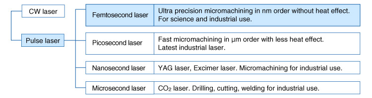
Lasers are broadly classified by operation as either continuous wave (CW) lasers that emit continuously, or pulse lasers that emit in pulses. The femtosecond laser is a pulse laser with pulse width of approximately 100 fs (1fs=10-15s). As the pulse duration is extremely short, it is also called the ultrashort pulse laser. When used for material processing, it is possible to perform nanometer-order ultra-precision fabrication without heat effects.
Position of femtosecond lasers
Advantages of femtosecond laser micromachining
The femtosecond laser has two main advantages compared to longer pulse lasers.
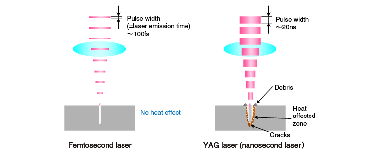
1. It is possible to process without heat effect, since the energy deposition time is extremely short
As the femtosecond laser has a pulse duration of ∼100fs (1fs=10-15s), exposure to the laser is finished before the heat can be transmitted to the material. Therefore it is possible to process material without causing heat-induced cracks or debris (substances melted or vaporized by the laser that readhere to the material surface). In contrast, using a YAG laser, which has a longer pulse duration of ∼20ns (1ns=10-9s), results in a heat-affected zone and cracks around the laser-treated area. The difference in pulse time between these two lasers can be further understood in terms of distance traveled; a 100fs pulse and 20ns pulse will travel 30μm and 6m, respectively.
2. By using a focusing lens to obtain high laser intensity, the microstructure can be formed solely in the area of the focal point.
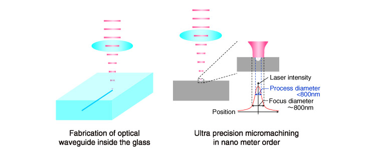
The wavelength of the femtosecond laser is 800nm, which is not strong enough to cause adsorption on transparent materials like sapphire and silica glass. However, since it is possible to obtain high laser intensity over 10TW/cm2 at the focal point, microstructures can be formed exclusively in the area of the focal point. By utilizing this feature, optical waveguide and microfluidics devices can be created inside the glass. As all materials (metal, semiconductor, glass, ceramics) can be processed with the femtosecond laser, it can be employed for drilling, cutting, and groove fabrication. Although generally the minimum diameter of the focused laser is approximately the same as its wavelength, by using the high intensity part of the laser, it is possible to fabricate nanostructures that are smaller than the laser wavelength. It is also possible to repair defects (chips and protrusions) in semiconductor photomasks.
Features of Orbray's femtosecond laser micromachining
We have been using laser processing for many years to cut diamonds in the production of diamond styluses, as well as to drill sapphire, ruby and ceramics. Since customer requests for smaller diameter holes have increased in recent years, we introduced the femtosecond laser earlier than other manufactures in order to provide ultra-precision micromachining. This has enabled us to process nanometer-order ultra-precision structures on transparent materials like sapphire and silica glass.
Our company's core technology (cutting, grinding and polishing) has been built on processing hard materials, and we can offer you the best solutions for materials such as silica glass, sapphire and ceramics. Our technology is practical for industrial-use semiconductors and micro-optics, as well as for bio-research. Since the optimal dimension range for micromachining (0.5µm to 25µm) is similar to cell sizes, there are unique applications such as microscope monitoring of cell membranes, cell trapping and micro fluidic devices.
Position of the femtosecond laser among other microfabrication technologies
This table compares femtosecond laser micromachining with other microfabrication processes. For the purposes of comparison, the example used in the table is micro-hole processing in silica glass, which has been frequently used for biology research needs.
Microfabrication processes |
Minimum diameter |
Maximum aspect ratio (length/diameter) |
Surface roughness |
Damaged area by processing |
|---|---|---|---|---|
Drilling | 150μm | 4∼20 |
Rough |
Exist |
Ultrasonic processing | 150μm |
3∼4 |
Rough |
Exist |
Sand blast | 100μm |
1∼1.5 |
Rough |
Exist |
UV laser | 25μm |
20 |
Rough |
Exist |
Femtosecond laser | 0.5μm |
100 |
Smooth |
None |
Dry etching | 0.01μm |
5 |
Very smooth |
None |

Silica glass is a brittle material that breaks easily, and it is generally difficult to form micro-holes in it - especially holes with a diameter less than 25µm. When it comes to mechanical drilling, the drill itself is hard to create, and the smallest possible diameter is only 150µm. Moreover multiple holes cannot be fabricated consecutively due to the frictional wear on the drill. Ultrasonic processing and sand blasting also have difficulties in creating micro-holes because of limitations in tool fabrication and mask durability; damage such as micro cracks often occurs around the hole surface. Although a 25µm hole can be produced with a UV laser, the silica glass is often broken by the thermal shock. Dry etching can create extremely small nano-holes, but due to the limits of photoresist's durability, the maximum hole depth is limited to 5 times the hole diameter. Moreover, since engineering designs change frequently during the prototyping stage, the additional photomasks required for each change add to the initial cost.
Orbray has addressed these issues by developing an in-house femtosecond laser micromachining system. By combining this system with our company's core technology of cutting, grinding, and polishing hard-to-process materials, we are able to manufacture ultrafine holes that cannot be produced by other processing methods. Our process for micro-hole fabrication offers the advantages of an optimal diameter range from 0.5 to 25µm, maximum aspect ratio of 100, smooth surface finish (surface roughness Ra is approximately 0.01µm), and not causing damage around the hole. Although laser process optimization is required, items such as photomasks are not needed.
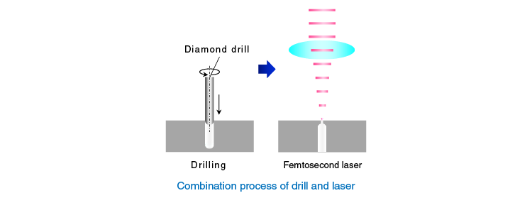
The femtosecond laser can achieve extremely fine and clean processing, but it is generally considered too inefficient and expensive for mass production. However, we have overcome this problem by using a combination of processing techniques. We use mechanical processing for the removal of large volume and use femtosecond laser micromachining only for micro fabrication. In this way, we have successfully employed the femtosecond laser in mass production processing. As an example, for thick samples, we have established the following combination drilling method: Using our in-house diamond drill, the large diameter hole is created partway through the material, and then the micro-/nanometer order hole is formed from the other side by the femtosecond laser.
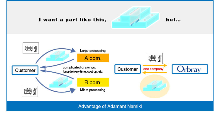
In addition to micro-hole processing, we can fabricate the sample itself, saving customers time and money by reducing the number of manufacturers needed to create a complete sample piece.
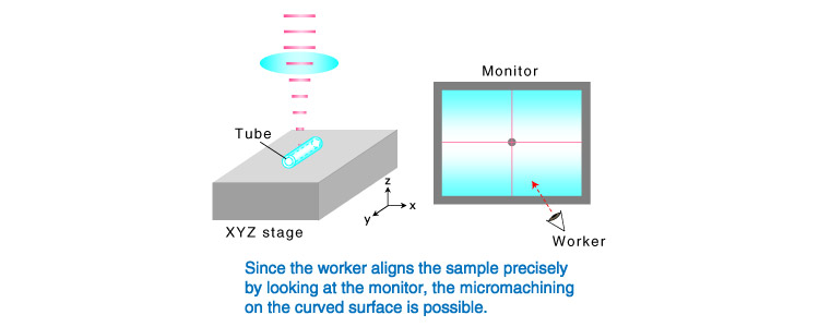
We can even process micro-holes on non-flat samples like tubes and grooves by using the CCD image to precisely align the sample and laser.
 We have received many requests from customers regarding micro processing of transparent materials like silica glass and sapphire, and have a good track record of producing both engineering samples and mass production quantities. We work with our customers starting from the design stage, to test samples, to mass production. Please do not hesitate to contact us for your micromachining needs.
Applications and examples
Ultra-precision nano-holes
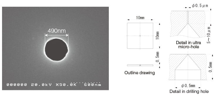
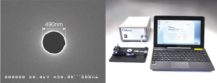
Ultra micro-hole, φ490nm, in the silica glass plate. Used for protein analysis. Using our in-house diamond drill, φ0.5mm hole is created partway through the material, and then the φ490nm hole is form the other side by the femtosecond laser. Used for protein analysis.
Precision micro-hole array
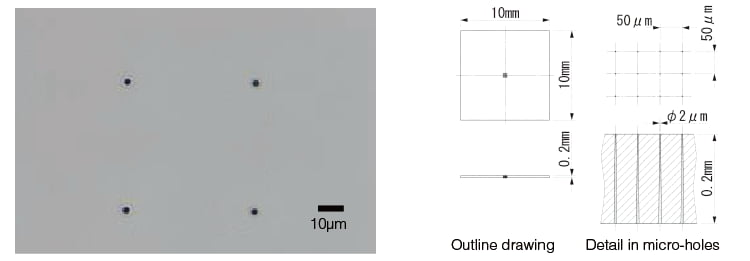
φ2μm micro-holes in a silica glass plate. Used for observing cell membranes. (We have developed a cell membrane monitoring device. Please refer to the following application product.)
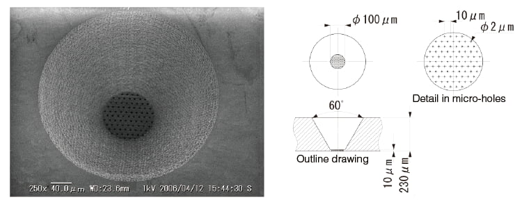
Hemispherical recess and through-hole combination
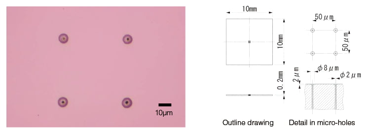
φ8μm hemispherical recess with φ2μm through-hole in a silica glass plate. Used for immobilization and observation of liposomes.
Numerous through-hole array
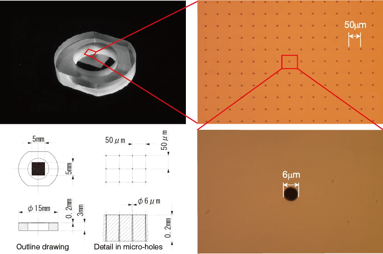
10,201 φ6μm micro-holes in a silica glass block. The block thickness is 3mm for increased strength and the thickness of the micro-hole array is 0.2mm. Used as a filter.
Micro-hole array in a glass tube
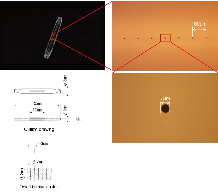
φ7μm micro-holes in a silica glass tube. Holes can be precisely processed, even on specialty shapes like glass tubes. Used for liquid flow.
Combination processing of a thick glass block
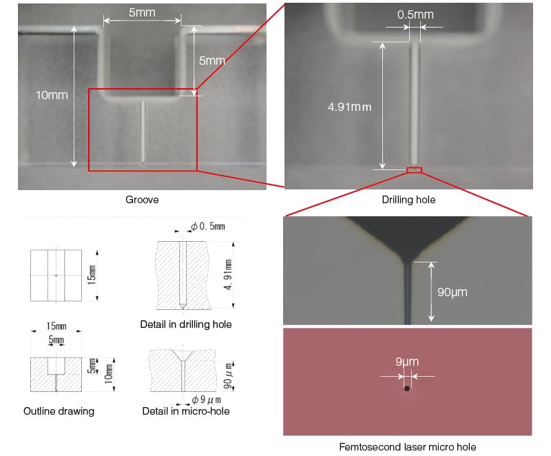
A groove, a drilled hole, and a femtosecond laser micro-hole in a 10mm thick silica glass block. With thick materials, the micro-hole can be created via the combination of machine and laser processing. Used for high-pressure liquid flow.
Micro-hole array
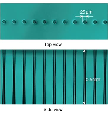
φ25μm micro-holes in a silica glass plate. Used as micro flow channels.
Tapered micro-hole
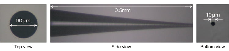
Tapered micro-hole in a silica glass plate. Dimensions measure φ90μm at the top, φ10μm at the end, and 0.5mm in length. The taper angle can be adjusted from 0 to 10 degrees. Used as a micro nozzle.
Y-shaped micro-hole
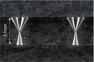
Y-shaped micro-hole in a silica glass block. Shapes that are difficult to machine can be processed with a laser. Used as a micro-channel.
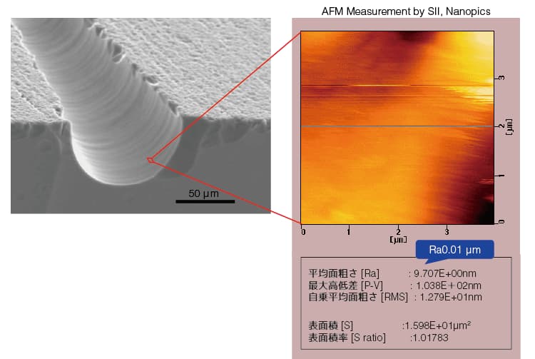
Surface roughness of the micro-hole
In the case of the silica glass, the average surface roughness is 0.01μm. It is very smooth and mirror like surface.
Three-dimensional microstructure in a sapphire
After a 60-degree tapered hole is created in the sapphire plate, φ2μm micro-holes are produced. Utilizes sapphire's hydrophobic properties to fix lipid bilayer membranes.
Nano-periodic structure in ceramic
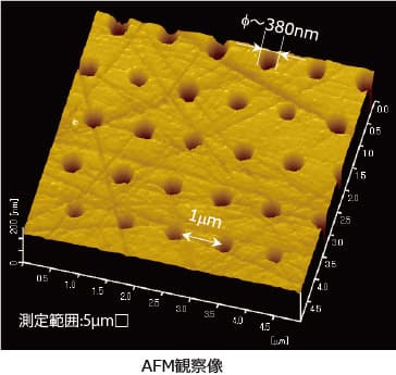
φ380nm nano dots in a ceramic plate. Used for optical applications.
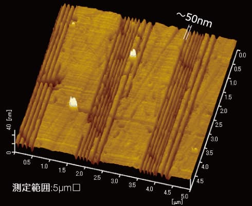
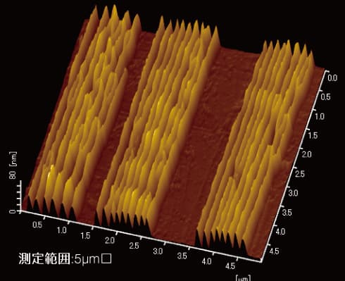
Nano-periodic structures mold of silica glass
Left: the nano-periodic structure mold formed in silica glass. The groove width and depth are 50nm and 5nm, respectively.
Right: a sample transferred onto resin.
Applied product (born from the needs of a researcher!)
Cell membrane observation device
This product was born from the needs of a researcher who wanted to fix and observe cell membranes by using φ2μm micro-hole array in the silica glass. (This development is a collaboration with Associate Professor Takashi Okuno, Faculty of Science, Yamagata University.) By fixing cell membranes on a micro-hole array via suction, quantitative analysis of membrane protein can be done on an extremely tiny sample. The following video shows the actual images of HeLa cell membranes using the observation device and a fluorescence microscope.
Provided by Associate Professor Takashi Okuno, Faculty of Science, Yamagata University
There are also other various applications in bio-research. This video shows fixing and observation of Tetrahymena.
Provided by Associate Professor Kentaro Nakano, Graduate School of Life and Environmental Sciences, University of Tsukuba
If you want to test the cell membrane monitoring device, please contact us. The demonstration kits are ready to use. You can also customize micro-hole designs.

